Research Overview
Vertically Aligned Nanocomposite (VAN) thin films
VAN thin films
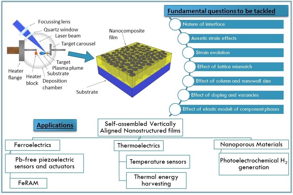
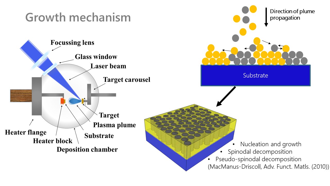
Vertically Aligned Nanocomposite (VAN) thin films comprise nanocolumns of one material embedded in another. These films are typically grown in a self-assembled manner by Pulsed Laser Deposition (PLD). The target used for PLD itself contains the two phases desired in the VAN thin films. The phases need to satisfy certain requirements such as immiscibility, thermal stability and some degree of lattice coherency with the substrate they are to be grown on. The growth process is shown schematically below.
Shown below are cross-sectional and plan-view STEM images of SrTiO3-Sm2O3 VAN thin films grown on SrTiO3 (001) single crystal substrates.
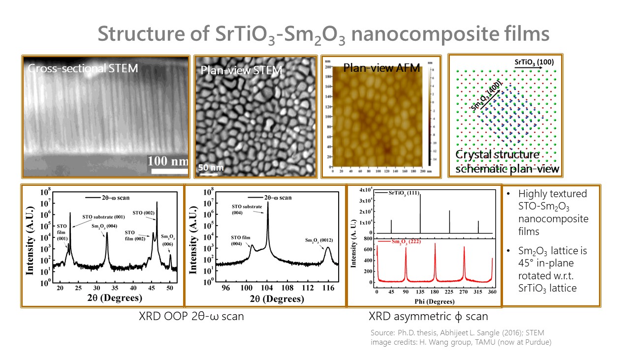
Given the natural coherence between SrTiO3 from the nanocomposite film and the substrate, the SrTiO3 phase grows with the same orientation as the substrate. On the other hand, Sm2O3 phase minimises lattice mismatch with SrTiO3 when it is grown with a 45° in-plane rotation w.r.t. SrTiO3 substrate and in (00l) out-of-plane orientation.
Thus, both SrTiO3 and Sm2O3 phases grow in (00l) orientation. This can be easily verified from out-of-plane 2θ-ω XRD scans and asymmetrical φ XRD scans and explained using the lattice-model showing coherence in Sm2O3 and SrTiO3.
The nanocolumns are of diameter ~15 nm and are spaced ~5 nm apart. A simple back-of-the-envelope calculation shows that this would be ~1012 nanocolumns/in2.
Ferro & Piezoelectric
VAN thin films can be used to enhance the ferroelectric/piezoelectric properties by strain-tuning at the vertical interface between the matrix and nanocolumnar phase. Vastly improved ferroelectric Curie temperature in SrTiO3 was shown by making it ferroelectric up to > 300 °C in SrTiO3-Sm2O3 VAN thin films.
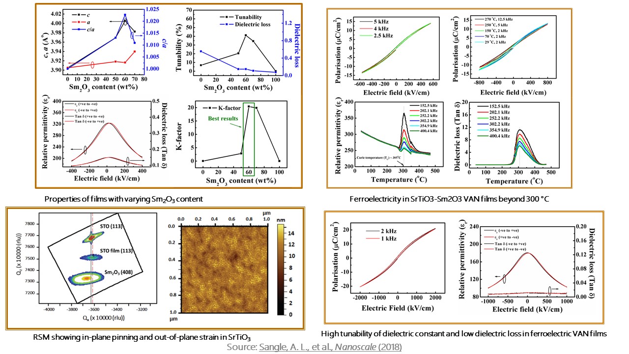
As seen in Fig. 3, the improved ferroelectric properties in VAN thin films led to the realisation of ferroelectricity in them, which in turn, led to highly enhanced tunability of dielectric constant with applied DC field whilst maintaining low dielectric loss, when measured at 1 MHz.
ReRAM in VAN Films
Memristor or Resistive Random Access Memory (ReRAM) is a type of computer memory technology in which the data is stored in the form of different resistance states of matter, which can be switched to or from by application of a DC bias.
In oxides, the most commonly accepted mechanism of switching between resistance states is the formation or breaking of conduction channels formed by oxygen vacancies. Typically, the resistive switching property is 'activated' by a so-called 'forming' process which causes soft dielectric breakdown of material by creating oxygen vacancies in it. As the process of forming is inherently stochastic in nature, controlling the concentration of oxygen vacancies and their distribution is difficult and not reproducible, leading to large variation in performance.
This problem of random generation of oxygen vacancies is bypassed if the oxygen vacancies can be engineered in number and position inside the sample.
VAN thin films consisting of two oxides such as SrTiO3 and Sm2O3 provide this unique opportunity by creating lattice discontinuities at the vertical interface. Shown below is a lattice model depicting this interface. We can see that every 11th oxygen plane in a Sm2O3 lattice in (00l) is in good coherence with every 8th oxygen-containing plane in SrTiO3 lattice, whereas between these two coherent planes there is a discontinuity.
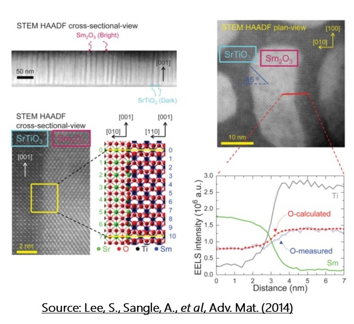
The formation of oxygen vacancies is confirmed by EELS study in which discrepancy between measured and calculated oxygen vacancies was compared.
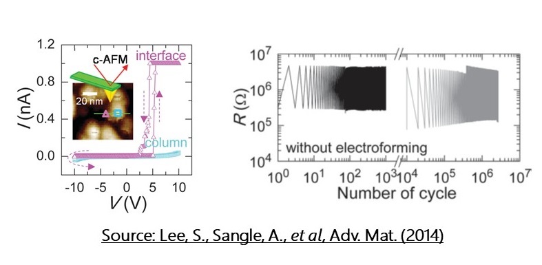
IV spectroscopy studies at the vertical interface and the nanocolumns show that hysteresis in IV characteristics can be found at the vertical interface only, confirming oxygen-vacancy mediated resistive switching. Further, endurance studies indicate a constant resistive switching performance between a high and a low resistance states for >106 cycles.
Photoelectrochemical water splitting
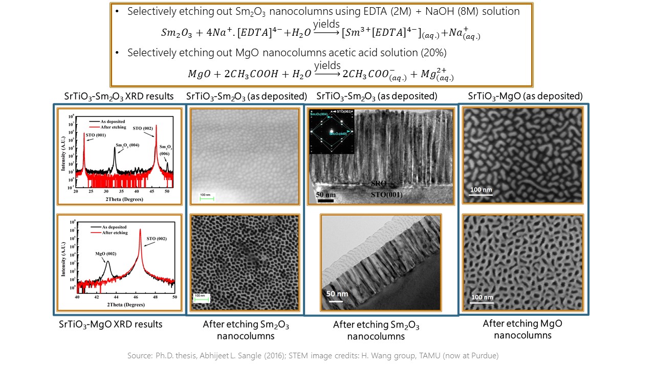
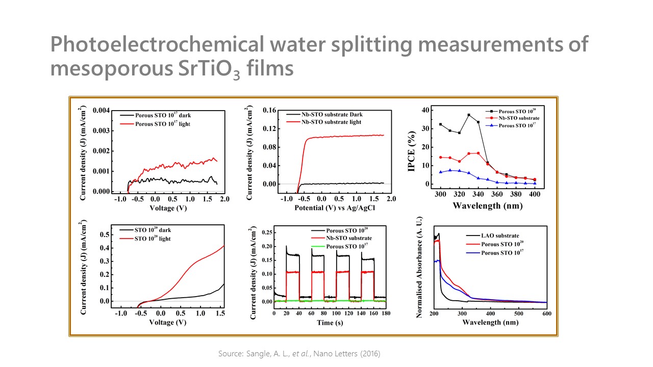
Presence of arrays of densely packed nanocolumns in VAN films (~1012 nanocolumns/in2) provides an opportunity to form extremely high surface area films if one of the two phases from the nanocomposite film can be selectively etched out.
We managed to selectively etch out Sm2O3 and MgO nanocolumns from their VAN films with SrTiO3, keeping the SrTiO3 matrix intact.
Epitaxial Free-standing Membranes
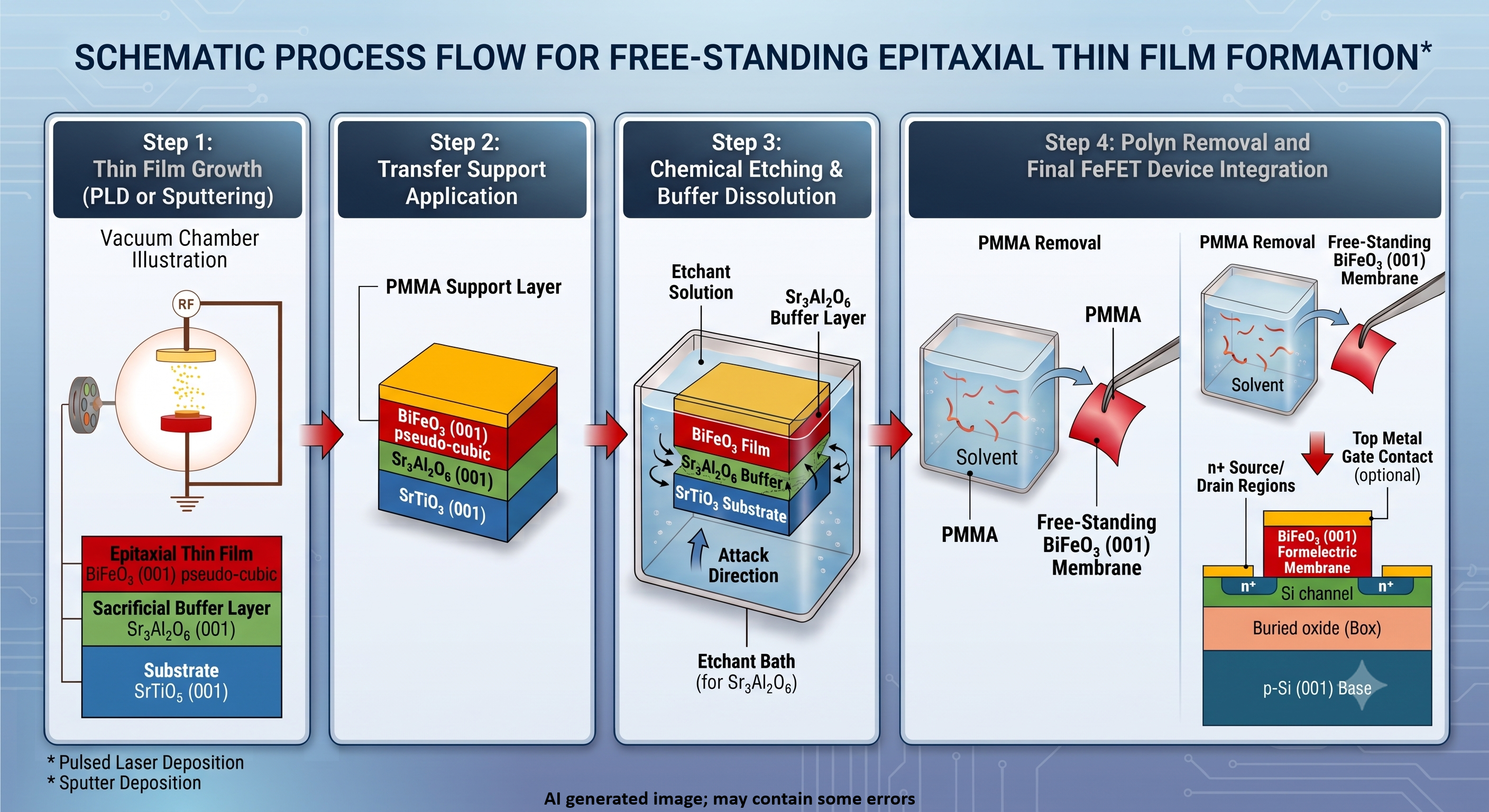
We are exploring the fabrication of epitaxial free-standing membranes. The process typically involves thin film growth, support application, selective chemical etching of a sacrificial buffer layer, and final device integration.
Printed Electronics
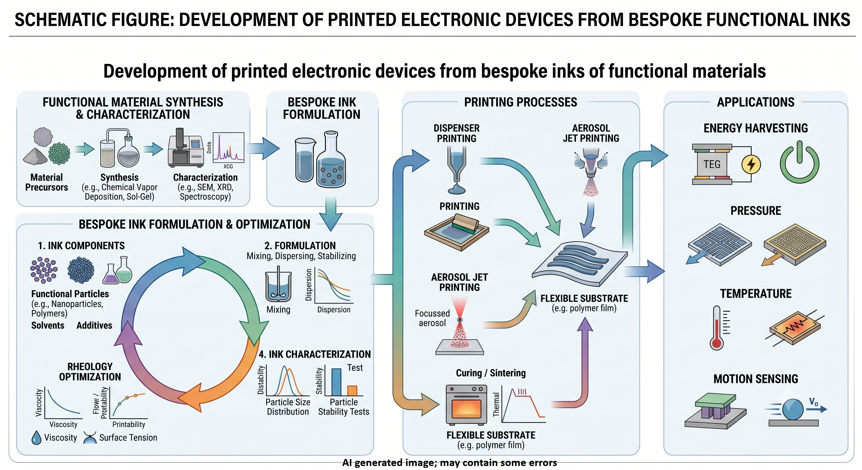
Our research in printed electronics spans the entire device fabrication lifecycle. This includes the synthesis and characterization of functional materials, the formulation and rheological optimization of bespoke inks, and the deployment of these inks using advanced printing processes such as aerosol jet and dispenser printing onto flexible substrates.
We aim to develop a range of applications such as energy harvesting devices, pressure sensors, temperature monitors, and motion sensors.
Piezoelectric Microelectromechanical Systems (MEMS) Devices
Research in Progress
Details about our work on piezoelectric MEMS devices will be updated here soon.